
2D 异质结
货号:105842 编号:XFG31
CAS号: 规格:SiO2/Si基底
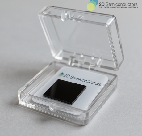
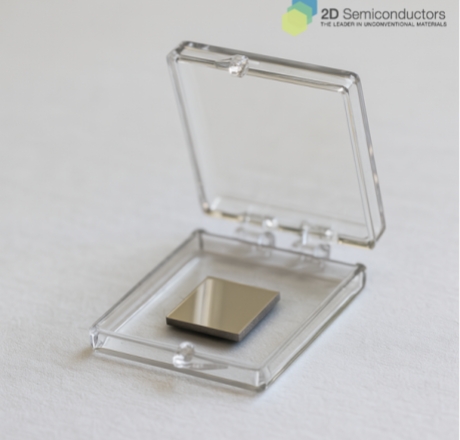
包装:WSe2/MoS2- Large area(~1cm) 保质期:90天
保存条件:常温干燥避光密封保存
产品名称
中文名称:2D异质结
英文名称:2D Heterojunctions
性质
美国2D公司进口的定制产品,询价请提供相关信息
2D研发团队已开发出可扩展的方法,将二维化学气相沉积(CVD)生长薄片背靠背转移,从而构建二维垂直异质结。尽管二维半导体研发团队采用无化学试剂转移工艺,仍可预期观察到转移过程(应变、衬底及缺陷)对二维薄膜物理特性的影响。鉴于生产流程的定制化特性,所有转移CVD产品均属最终销售且不可退款。
本产品展示了2D公司在多种基底与异质结结构领域的技术实力。定价主要取决于基底类型、CVD单层厚度以及您应用场景和样品规格带来的特定技术挑战。

其他信息
原链接:https://2dsemiconductors.com/2d-heterojunctions/
Frequently asked questions
Q1: Can you make any vertical heterojunctions?
A: We can place any CVD materials offered by our company onto each other to create bilayers as well as trilayers.
Q2: Can you make Moire pattern samples?
A: When 2D triangles are placed on top of other 2D triangles, they create 2D Moire lattices. However, these lattices will have random angles, varying from small to large twist angles. We advise clients to characterize each individual twisted triangle using second harmonic measurements to precisely identify the twist angles. Our company does not offer Moire lattices with identified twist angles due to the specialized toolsets needed and the impractical nature of manufacturing them.
Q3: Can you transfer monolayers onto TEM grids?
A: Yes, we can transfer any CVD product onto any TEM grids. Our company requires you to select your own TEM grids, inform us the model, and send (extra) TEM grids so that we can do tests to deliver you good quality samples.
Q4: Can you guarantee that CVD monolayers will be same quality after the transfer?
A: Transfer process requires polymeric stamping and / or chemical processes. These steps generally will introduce some cracks and voids in the samples. But if you selected to transfer full area CVD monolayers, they will still be at large scales. There might be some folding, wrinkling effects, and this is normal. If your CVD monolayer is luminescent, after the transfer optical properties will remain similar with PL emission at the same wavelenghts
Q5: What kind of substrates can you transfer onto?
A: You would be surprised to know but we have transferred CVD monolayers more than 100 different substrates to date. Examples include, Bragg reflectors, plasmonic structures, SiO2/Si, sapphire, quartz, mica, PET, polymer, other 2D materials, glass, TEM grids, metals, and even on a diamond!
Q6: What is the typical processing times?
A: This will depend on your project, chemistry required, and your sets of requirements towards sample production. It is typically around 1-3 weeks.
江浙沪皖用户邮费为10元,其他地区用户邮费为20, 国际运费请咨询sales@xfnano.com。购买满 500.0 元免运费。如果库存显示为0, 请电话或邮件和销售确认,免费热线电话:400 025 3200邮件:sale@xfnano.com 感谢您的支持!